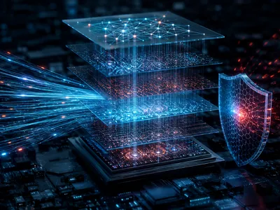
Why Neuromorphic Design Replaces Memory Bottlenecks?
The fundamental departure of neuromorphic engineering from classical computing lies in its rejection of the von Neumann architecture. This decades-old paradigm, which separates the central processing unit from memory, creates a bottleneck known as the memory wall. Data must be shuttled back and forth continuously, consuming immense energy and limiting true parallel processing.
Neuromorphic chips address this inefficiency by adopting a brain-inspired, in-memory computing model. Computation occurs directly within a dense network of artificial synapses, drastically reducing data movement. This architectural shift is not merely an incremental improvement but a foundational rethinking aimed at achieving the brain’s remarkable efficiency in pattern recognition, sensory processing, and adaptive learning.
How Do Spikes Replace Binary Code?
At the heart of neuromorphic computation lies the spiking neural network (SNN), which abandons the continuous, high-precision values of artificial neural networks. SNNs communicate via discrete, event-driven pulses called spikes, mimicking the action potentials of biological neurons. Information is encoded not in the amplitude of a signal but in the precise timing and frequency of these spikes.
This temporal coding scheme offers profound advantages. It inherently exploits the sparsity found in real-world sensory data; nothing is computed when there is no event. This leads to a significant reduction in power consumption, as energy is expended only during spike generation and propagation, unlike traditional processors that constantly clock data.
The communication paradigm fundamentally shifts from broadcast to addressing. In a conventional CPU, results are written to a shared memory location for any other unit to read. In a neuromorphic system, a spike is a directed message sent only to specific downstream neurons along configured synaptic pathways, enabling massively parallel and event-driven processing without a global memory bus.
How Silicon Hardware Replicates Synaptic Memory?
The physical instantiation of neuromorphic principles requires a hardware blueprint composed of two fundamental units: artificial neurons and synapses. Silicon neurons are circuits designed to emulate the leaky integrate-and-fire behavior of biological cells, integrating incoming currents until a threshold triggers a spike. More complex models can replicate adaptive thresholds or bbursting behaviors, but they trade biological fidelity for circuit area and power.
Synaptic arrays form the core memory and computational fabric. Each crosspoint in a network represents a programmable synaptic weight, stored as conductance in a non-volatile memory element. Vector-matrix multiplication, the fundamental operation of neural networks, occurs naturally via Ohm’s law and Kirchhoff’s law when input voltages are applied to rows and the resulting column currents are summed, achieving in-memory computation.
Two dominant architectural approaches have emerged in implementing these components, each with distinct trade-offs between flexibility, density, and efficiency.
| Architecture | Core Principle | Advantages | Challenges |
|---|---|---|---|
| Digital Asynchronous | Uses custom digital logic and event-driven packet routing to emulate spiking networks. | High precision, programmability, and scalability with advanced CMOS nodes. | Higher static power, less energy-efficient per synaptic event than analog. |
| Mixed-Signal Analog | Exploits the physical properties of transistors (sub-threshold operation) to emulate neural dynamics. | Ultra-low power consumption, native implementation of temporal dynamics. | Susceptible to noise and fabrication variability, less flexible. |
Why Non-Volatile Materials Power Compact Synapses?
While CMOS technology underpins most current neuromorphic chips, extending beyond traditional silicon is essential for achieving high density and energy efficiency. Emerging non-volatile memory technologies, known as memristors or resistive random-access memory (RRAM), are pivotal. Their conductance can be precisely modulated by electrical history, making them ideal, compact analogs for synaptic weights.
Research focuses on materials like hafnium oxide, tantalum oxide, and phase-change materials (e.g., GST). These materials enable the creation of dense crossbar arrays where computtion occurs at the location of data storage with unprecedented parallelism. Their inherent non-volatility and analog programmability are critical for on-chip learning and reducing static power to near zero.
The exploration of novel materials systems is not limited to synapses. Ferroelectric field-effect transistors (FeFETs) are being investigated for implementing neurons with intrinsic memory, while organic electronic materials offer potential for flexible, bio-integrated neuromorphic systems. The material innovation pipeline is a primary driver for next-generation neuromorphic scale and capability, moving from mere emulation to true physical isomorphism with neural processes.
The following list highlights key material classes and their primary functional role in neuromorphic hardware.
-
SynapseTransition Metal Oxides (HfO2, TaOx)Used in memristive synapses for analog weight storage and stochastic switching.
-
SynapseChalcogenides (GST)Phase-change materials offering multi-level conductance states for synaptic plasticity.
-
Neuron/SynapseFerroelectric Perovskites (HZO)Provide non-volatile polarization for FeFET-based neurons and synapses.
-
InterfacingOrganic Mixed Ionic-Electronic ConductorsEnable bio-compatible, low-voltage devices that mimic biological ion channels.
Can Neuromorphic Processors Upgrade Edge Sensing?
Neuromorphic computing is transitioning from laboratory research to tangible deployment, with edge sensing being its most immediate domain. Dynamic vision sensors (DVS), which output sparse spikes only for pixel-level changes, are naturally paired with neuromorphic processors. This combination enables real-time object tracking and gesture recognition at milliwatt power budgets, impossible for standard frame-based systems.
In autonomous systems, this technology offers robust, low-latency perception. Neuromorphic chips can process multi-modal sensory data—visual, auditory, tactile—in a unified event-based framework, facilitating quicker decision-making in unpredictable environments. This is critical for robotics operating in energy-constrained or remote settings.
The reach of these systems extends to extreme environments where reliability and power efficiency are paramount. Satellite onboard processing for earth observation can utilize neuromorphic chips to identify features like cloud cover or wildfires directly at the source, drastically reducing the volume of data downlinked. Similarly, biomedical implants for neural signal processing benefit profoundly from the ultra-low power continuous operation of spiking architectures.
The following table illustrates the transformative impact across diverse sectors, highlighting the core advantage driving adoption in each.
| Application Sector | Specific Use Case | Neuromorphic Advantage |
|---|---|---|
| Mobile & Edge AI | Always-on voice/gesture interfaces, keyword spotting. | Microwatt power consumption enables perpetually active sensing. |
| Robotics & Drones | Autonomous navigation, collision avoidance in dynamic settings. | Sub-millisecond latency for real-time reaction to events. |
| Biomedical Devices | Closed-loop neuroprosthetics, epileptic seizure prediction. | Energy efficiency for implantable, long-term operation. |
| Space & Defense | On-satellite data filtering, radar signal processing. | Radiation tolerance (inherent or designed) and extreme efficiency. |